Overview: Two Versions
The Cinematronics RAM Test runs continual tests on the three RAM chips on a Cinematronics or Vectorbeam CPU board and will operate regardless of any bad RAM on the board.
There are two versions of the Cinematronics RAM test, each with its own advantages and disadvantages. One version outputs the test results to the vector monitor. The other outputs the test results to the connector J4, which normally connects the CCPU board to the game's audio board.
Monitor Output Version Advantages:
- Results can be easily seen displayed on the vector monitor - no additional equipment required.
- Display shows if a RAM chip has an output stuck high or low.
- Requires no working RAM to operate.
Monitor Output Version Disadvantages:
- Requires a working vector monitor connected to the CCPU to view result of tests.
- Only tests memory locations $00 and $FF. Test will find RAM with bad outputs but not a RAM chip with bad individual RAM bits that are not within these two memory locations.
J4 Output Version Advantages:
- Results are read individually using a logic probe or all at once using a small circuit board connected to J4. No vector monitor is required, but it can be attached while the test is running.
- Does initial test on RAM location $00. If it passes, the RAM test runs complete tests of the CPUs 256x12-bit memory locations.
- Requires no working RAM for initial test to operate.
J4 Output Version Disadvantages:
- Requires a a logic probe or additional hardware to read test results.
- Does not display an indication whether a RAM chip's outputs are stuck high or low.
- For full test of RAM, requires RAM location $00 to work correctly (the first 4-bits in each of the CPUs three RAM chips).
RAM Test ROMs Installation
- Burn 2716(2x2k) or 2732(2x4k) version to two EPROMs appropriate for the board you will be testing.
- Confirm game is OFF and remove current ROMs in P7 and T7.
- Install RAM Test ROMs into P7 and T7.
- Unplug power to sound PCB: the program has no capability to control it.
- If using the J4 output version, remove the ribbon cable at J4, noting orientation for later reconnection. Connect RAM Test PCB if you are using one, otherwise connect logic probe to the CCPU under test.
- Turn on power, confirm program is operating by observing the brief flash of the reset LED and consult vector display or J4 connector pins for continual test results.
- IF the reset LED stays lit, immediately turn off power and troubleshoot cause.
Using RAM Test With Monitor Output
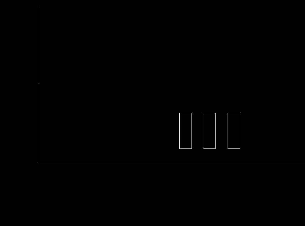
The RAM test draws a visual representation of the CPU's RAM chips on the vector display. It uses $005 (0101), $00A (1010), $050, $0A0, $500, and $A00 as test data, testing memory locations $00 and $FF.
It should run on all Cinematronics monitors:
- Bi-Level at High Intensity
- 16-Level Intensity(Sundance) at High Intensity
(MAME OK, actual hardware confirmation needed) - 64-Level Intensity (Solar Quest) at Low Intensity
(MAME OK, actual hardware confirmation needed)
There are no adjustments for the mirror on Solar Quest machines. The image will appear reversed.
Displays and Limitations

- Display if all RAM pass tests.

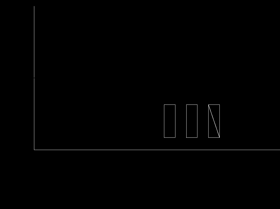
- Bad chips display a forward slash / if a bit stuck low error is found
(0 was found where there should have been a 1)

- Bad chips display a backward slash \ if a bit stuck high error is found
(1 was found where there should have been a 0)

- All three chips display an X if the program determines it can't reliably test the RAM.
(See below for more info)
| Test Result | Test Display | Notes | |||||
|---|---|---|---|---|---|---|---|
| N14 | M14 | L14 | N14 | M14 | L14 | ||
| OK | OK | OK | [] | [] | [] | ||
| 0 Found, Expecting 1: | |||||||
| 0 | OK | OK | [/] | [] | [] | ||
| OK | 0 | OK | [] | [/] | [] | ||
| OK | OK | 0 | [] | [] | [/] | ||
| 0 | 0 | OK | [/] | [/] | [] | ||
| OK | 0 | 0 | [] | [/] | [/] | ||
| 0 | 0 | 0 | [/] | [/] | [/] | ||
| 1 Found Expecting 0: | |||||||
| 1 | OK | OK | [\] | [] | [] | ||
| OK | 1 | OK | [] | [\] | [] | ||
| OK | OK | 1 | [] | [] | [\] | ||
| 1 | 1 | OK | [\] | [\] | [] | ||
| OK | 1 | 1 | [] | [\] | [\] | ||
| 1 | 1 | 1 | [\] | [\] | [\] | ||
| 1 | 0 | OK | [X] | [X] | [X] | Can't Reliably Test | |
| 1 | OK | 0 | [X] | [X] | [X] | Can't Reliably Test | |
| etc... | |||||||
0 fails display all chip failures.
1 fails display all chip failures.
1 fails with any 0 fails - possible false readings: program draws can't reliably test display.
This limitation is because it's not possible to isolate (via ANDing or Bit-Shifting) an individual 4-bit section of a 12-bit data read. Bits stuck high or low in a 4-bit section not being tested would produce a false failure in the chip being tested.
Using RAM Test With J4 Output
The RAM test outputs the results of testing the CPU's ram chips to the J4 connector as shown above. It uses $005 (0101), $00A (1010), $050, $0A0, $500, and $A00 as test data, first for memory locations $00 and $FF. If these locations pass then these values are written and verified for all memory locations.
J4 Pin out
| Top of CCPU | |||||||||
|---|---|---|---|---|---|---|---|---|---|
| 1 | 2 | 4 | 6 | 8 | 10 | 12 | 14 | 16 | |
| 1 | 3 | 5 | 7 | 9 | 11 | 13 | 15 | ||
J4 RAM Test Usage
| Top of CCPU | |||||||||
|---|---|---|---|---|---|---|---|---|---|
| 1 | GND | N14 | M14 | L14 | |||||
| +5 | - | Full | Able | ||||||
J4 RAM Test Results
Use logic probe or RAM test PCB to read results.
Harness or CCPU [+5v]
Harness, CCPU or J4-08 [GND]
J4-12 [N14 Result]
- 0 Output = Active-high = Bad
- 1 Output = Active-low = Good
J4-14 [M14 Result]
- 0 Output = Active-high = Bad
- 1 Output = Active-low = Good
J4-16 [L14 Result]
- 0 Output = Active-high [Bad]
- 1 Output = Active-low [Good]
J4-11 Unused - Active Low
J4-13 Running Full Test of RAM
- 0 Output = Active-high = Not Running Full Test
- 1 Output = Active-low = Running Full Test
J4-15 Ability to Run RAM Tests
- 0 Output = Active-high = Can't Run RAM Tests
- 1 Output = Active-low = Can Run RAM Tests
Displays and Limitations
| Test Result | Test Display | Notes | ||||||||
|---|---|---|---|---|---|---|---|---|---|---|
| J4-12 | J4-14 | J4-16 | J4-11 | J4-13 | J4-15 | |||||
| N14 | M14 | L14 | N14 | M14 | L14 | - | Full Test | Can Test | ||
| OK | OK | OK | ||||||||
| 0 Found, Expecting 1: | ||||||||||
| 0 | OK | OK | ||||||||
| OK | 0 | OK | ||||||||
| OK | OK | 0 | ||||||||
| 0 | 0 | OK | ||||||||
| OK | 0 | 0 | ||||||||
| 0 | 0 | 0 | ||||||||
| 1 Found Expecting 0: | ||||||||||
| 1 | OK | OK | ||||||||
| OK | 1 | OK | ||||||||
| OK | OK | 1 | ||||||||
| 1 | 1 | OK | ||||||||
| OK | 1 | 1 | ||||||||
| 1 | 1 | 1 | ||||||||
| 1 | 0 | OK | Can't Reliably Test | |||||||
| 1 | OK | 0 | Can't Reliably Test | |||||||
| etc... | ||||||||||
0 fails display all chip failures.
1 fails display all chip failures.
1 fails with any 0 fails - possible false readings: program draws can't reliably test display.
This limitation is because it's not possible to isolate (via ANDing or Bit-Shifting) an individual 4-bit section of a 12-bit data read. Bits stuck high or low in a 4-bit section not being tested would produce a false failure in the chip being tested.
Building a RAM Test PCB
Building a Test PCB requires:
- (6) Red LEDs
- (6) Green LEDs
- (12) 470 ohm resistors*
- (1) 10uf electrolytic capacitor
- (1) 74LS244, 74ACT541 would be even better (has a different pinout)
- (1) Small Breadboard
- (6) Male/Female jumper wires (to connect breadboard to CCPU J4)
- (2) Wires to connect +5 and ground to the breadboard
- (1) Screw Terminal Block, 2 position, 5mm (optional to connect power wires to breadboard)
- Wires to connect points on the breadboard
* Please adjust these values based on the LEDs used, being conservative in their brightness and the resulting power draw.
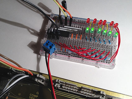
The board works like six identical logic probe circuits. The green LED lights on logic level low, the red on logic level high. The LEDs are all positioned so that the anode (longer leg) is on the left. Click on the image above to see a larger view of the circuit on the breadboard.
Please note that the power for the board should be taken from the game's harness and not from the J4 connector itself (there is no +5v source at J4). I'm using a pass-thorugh Molex connector with extra +5v and ground wires attached that connects to the game's harness.
If there is interest I can add a schematic to this page or possibly get a small run of PCBs made.
Donate or Purchase EPROMs:
By donating for your download or purchasing EPROMs, you can help support my work on these projects. Please choose from the options below:
Outerworld Arcade is in the process of moving.
During this transition I may not have access to my games
or tools
for testing code, building PCBs or burning EPROMs.
Please contact me before placing orders.
Download ROMs:
Disclaimer: These programs are provided AS-IS. I will not be held responsible for any damages caused by their use.
The binaries include the RAM test ready for use with either 2716 or 2732 EPROMs. The 2716 and 2732 versions are identical except for additional padding to accommodate the larger EPROM size.
Latest Releases:
Monitor Output v1.0 (01-01-2018) [Download Binary]
J4 Output v1.0 (12-09-2017) [Download Binary]
Project Background & Technical Information
I have been working on a RAM test for the Cinematronics hardware on and off starting in July 2009 through the initial release in January 2018. It was originally written for the Cinematronics Test ROM and then later spun off into its own project.
One of the challenges involved writing code for the CCPU that didn't require RAM to execute. When not using RAM, there are only two registers in the Cinematronics hardware that can be used as variables, a primary accumulator and a secondary accumulator. These are also used as the X and Y coordinates when drawing to the monitor.
This means that in the monitor display version of the RAM test no variables can be used.
In the J4 output version the secondary accumulator is not needed for draws and is available as our one variable to keep track if a test on a RAM chip was successful. If all three RAM chips pass their initial test on RAM location $00, we assume it is OK and use it to store a return address from a subroutine that tests one page of memory (16 bytes) with a value passed to it in the primary accumulator.
Another challenge was drawing to the vector monitor without using RAM. In all of the routines I have seen, RAM was used to do calculations during a vector draw. After deciding to pre-calculate the values and hard-code them, I ran into a problem.
Below is some code used to draw a line in the RAM test:
                                        ;---------------
                                        ; Position Beam
                                        ;---------------
badram1         bld(BAD1_X1)            ; X1
                sbld(BAD1_Y1)           ; Y1
_wait           lpai(_wait)
                jvn                     ; WAIT FOR VECTOR DRAW
                iv                      ; POSITION BEAM

                                        ;------------
                                        ; Delay: $80
                                        ;------------
                bld($F80)               ; A=$F80
_wait2          lpai(_wait2)
                a4i($1)
                jcz                     ; Loop Again if <> 000

                                        ;------------------
                                        ; Normalize Vector
                                        ;------------------
                bld(BAD1_DELTAX)        ; X2-X1
                sbld(BAD1_DELTAY)       ; Y2-Y1
                nv                      ; NORMALIZE VECTOR

                                        ;-------------
                                        ; Draw Vector
                                        ;-------------
                bld(BAD1_DRAWX)         ; Value from MAME($0A0) + X1($2F8) = $398
                sbld(BAD1_DRAWY)        ; Value from MAME($200) + Y1($100) = $300
                dv                      ; DRAW VECTOR
I found that executing the normalize vector (NV) command causes the value in each accumulator to be shifted to the left a number of times. In normal routines using RAM, the beginning XY values are added from RAM to whatever is stored in the accumulators after the NV command.
In order to get my hard-coded values to work properly, I had to run the code in MAME. By setting a breakpoint after each normalize vector command, I was able to get the value stored in the accumulators after this command. I could then add the beginning XY value to each to have my hard-coded values. I wasn't able to use a simple addition command because they either rely on RAM, or are only 8-bits in length, where 12-bit lengths are needed.
The hardware also seems to have a limitation on a vector's line length. One of the only times a line is drawn across the entire screen is in the diagnostic mode of Solar Quest. In this mode, the lines are drawn in two passes, one for each side of the screen. For the monitor output version of the RAM test, the outline of the CPU board is drawn using four lines, two in each direction. Further tests are needed to clarify the details of this limitation.
Below is an overview of the code for each version of the RAM test.
********************************
* Rom Overview: Monitor Output *
********************************

 Setup:
    Text: Name, Version, Date, Copyright, Author
    Set Intensity that is valid for Sundance, Solar Quest, Bi-Level Games
 Draw Screen:
    Draw Lower Board Edge
    Draw Left Board Edge
    Draw L14 Ram Outline
    Draw M14 Ram Outline
    Draw N14 Ram Outline
 Ram Test:
    Check if a memory bit is stuck on (Memory Location $00)- if so, goto those tests
    No bits stuck on:
        Test Ram L14 with $005 for bits stuck off (Memory Locations $00,$FF)
        Test Ram L14 with $00A for bits stuck off (Memory Locations $00,$FF)
            Draw BAD Line if a compare fails (/)
        Test Ram M14 with $050 for bits stuck off (Memory Locations $00,$FF)
        Test Ram M14 with $0A0 for bits stuck off (Memory Locations $00,$FF)
            Draw BAD Line if a compare fails (/)
        Test Ram N14 with $500 for bits stuck off (Memory Locations $00,$FF)
        Test Ram N14 with $A00 for bits stuck off (Memory Locations $00,$FF)
            Draw BAD Line if a compare fails (/)
        Goto Cold Start Inhibit
    A bit is stuck on:
        Check if a memory bit is stuck off (Memory Location $00)-
            if so, goto "Draw Can't Reliably Test"
        Test Ram L14 with $FF0 for bits stuck on (Memory Locations $00,$FF)
            Draw BAD Line if compare fails (\)
        Test Ram M14 with $F0F for bits stuck on (Memory Locations $00,$FF)
            Draw BAD Line if compare fails (\)
        Test Ram N14 with $0FF for bits stuck on (Memory Locations $00,$FF)
            Draw BAD Line if compare fails (\)
 Cold Start Inhibit
 Loop Again to Draw Screen

 Draw Can't Reliably Test
            Draw Bad Ram L14 Line (/)
            Draw Bad Ram M14 Line (/)
            Draw Bad Ram N14 Line (/)
            Draw Bad Ram L14 Line (\)
            Draw Bad Ram M14 Line (\)
            Draw Bad Ram N14 Line (\)
            Goto Cold Start Inhibit Routine

***************************
* Rom Overview: J4 Output *
***************************

Setup:
    Text: Name, Version, Date, Copyright, Author
    Return Beam to Screen Center
    Set all outputs to active-low

Ram Test Loop:
    Set up check for full test = 3 (3 RAM chips to check)
    Initial Ram Test:
        Test if A Memory Bit is Stuck ON - goto test 2 if so
        Test 1: Test if Memory Bits Can Be Off
            Test Ram L14 with $005 (Memory Locations $00,$FF)
            Test Ram L14 with $00A (Memory Locations $00,$FF)
                Set LEDs
                If Pass: subtract one from full test check
            Test Ram M14 with $005 (Memory Locations $00,$FF)
            Test Ram M14 with $00A (Memory Locations $00,$FF)
                Set LEDs
                If Pass: subtract one from full test check
            Test Ram N14 with $005 (Memory Locations $00,$FF)
            Test Ram N14 with $00A (Memory Locations $00,$FF)
                Set LEDs
                If Pass: subtract one from full test check
            Goto Full Tests

        Test 2: Test if a Memory bit is Stuck On
            Test if A Memory Bit is Stuck OFF - goto "Draw Can't Reliably Test" if so.
            Test RAM L14
                Set LEDs
            Test RAM M14
                Set LEDs
            Test RAM N14
                Set LEDs
            Goto Cold Start Inhibit

    Complete Ram Test:
        Test if we can run full tests (other tests were ok)
            Test Ram L14 with $005
            Test Ram L14 with $00A
                Set LEDs
            Test Ram M14 with $005
            Test Ram M14 with $00A
                Set LEDs
            Test Ram N14 with $005
            Test Ram N14 with $00A
                Set LEDs
            Goto Cold Start Inhibit

    Cold Start Inhibit Routine
    Loop Again (Forever)

    Draw Can't Reliably Test
        Set LEDs
        Goto Cold Start Inhibit Routine

    Subroutine: Test RAM


